ProjectsDesigning a Multi-stage Amplifier
Designing a Multi-stage Amplifier
A two-stage BJT amplifier (CE + CC) hand-derived and validated in Multisim against nine simultaneous specs - gain, input resistance, quiescent current, and a distortion-free swing.
Why it exists
A 2-week individual design project, with two scheduled check-ins to review progress. The brief wasn't "build an amplifier" - it was "build the one specific amplifier that simultaneously satisfies every line on this spec sheet," using only BJTs and parts from the course kit.
Everything it had to hit at once
Two stages, one circuit
A common-emitter stage does the actual amplifying; a common-collector stage after it does nothing but protect that gain from the load. CE was chosen over CB because CB doesn't handle a small source resistance well, and CE still allows emitter degeneration despite inverting the signal. CC contributes almost no gain of its own - its entire job is to keep RL from loading down what Q1 already built.
Vi
Rs = 600 Ω
Q1 - CE stage
2N3904 · RC 7.83kΩ · RE1 25kΩ
Q2 - CC stage
2N3904 · RE2 1.2kΩ
Vo
RL = 1kΩ
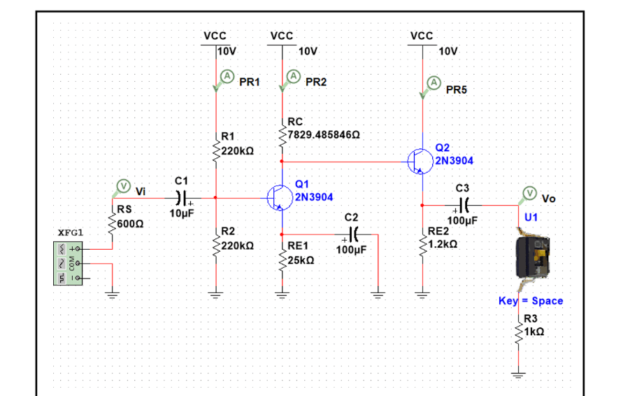
The actual Multisim schematic - Q1's CE stage on the left, Q2's CC stage on the right.
Component values, chosen not guessed
R1 = R2 = 220 kΩ
maxed out on purpose - makes IB negligible next to IR1/IR2, and since R1, R2 >> rbe, Rin = R1 || R2 || rbe collapses to just rbe
RE1 = 25 kΩ
raised specifically to push rbe1 (and therefore Rin) over the 20 kΩ floor - more emitter degeneration means lower Ic1, and rbe = βVT / Ic runs the other way
RC = 7,829.49 Ω
solved directly from Av = -gm x RC to land the no-load gain within 10% of the required 50
RE2 = 1.2 kΩ
chosen close to RL = 1 kΩ on purpose, so the emitter-follower's output resistance doesn't get dragged down once the load is actually attached
The scorecard
Expected vs. measured, straight from the final Multisim validation pass:
The one spec that didn't fully land
The output swing requirement - several volts peak-to-peak, no-load - came in well under target in simulation (closer to half a volt), even though the gain measured within tolerance. Solving for the exact source voltage that would hit the target swing produced a badly distorted waveform instead, so a smaller, distortion-free Vs was kept deliberately over one that hit the swing spec on paper. The report is upfront about the tradeoff rather than hiding it: fixing the swing needed more than adding another stage, since gain wasn't the actual bottleneck.
Solo work, using only parts from the course's ELE404 kit. Everything above was hand-derived first - small-signal analysis, KCL/KVL on the biasing network, solving for rbe and gm - and then checked against Multisim before anything was called finished.
© 2026 Gaurav Divecha. All rights reserved.